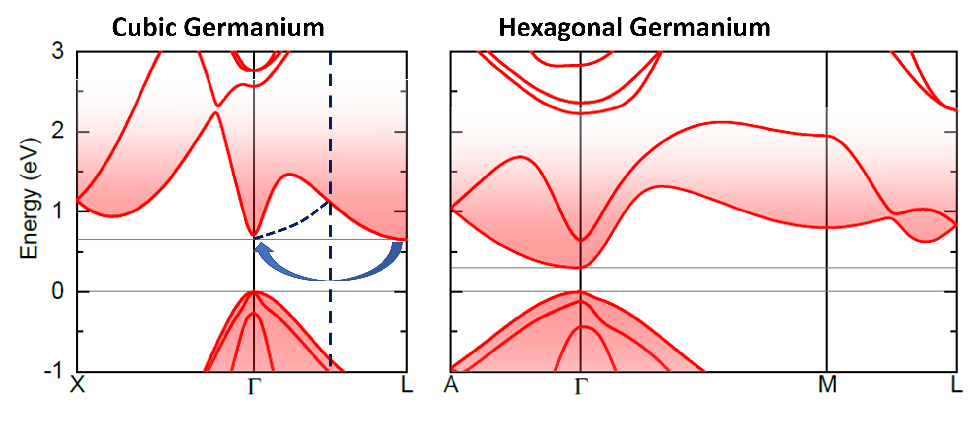
The hexagonal crystal polytype SiGe (Hex-SiGe), as pioneered by the SiLAS consortium, a predecessor of the Opto Silicon consortium, recently emerged as a new direct bandgap semiconductor. This is seen in the Figure on the right and published in this Nature paper.
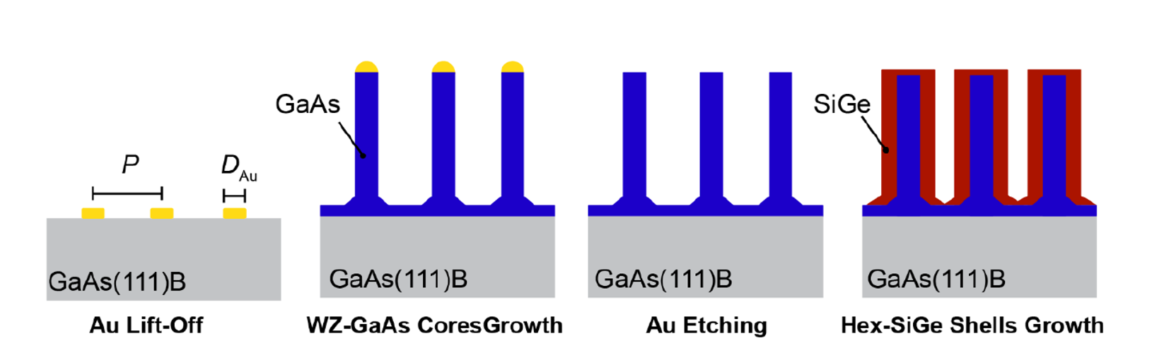
The core nanowire growth starts with a GaAs (111)B substrate patterned with Au catalyst seeds, which is introduced in the MOVPE reactor and annealed at a temperature higher than the eutectic temperature forming an alloy between the catalyst seed and the substrate. Next, the GaAs gas precursors (TMGa and AsH3) are introduced, and Au-catalysed GaAs core nanowires are grown. To proceed with the SiGe shell growth, Au seeds are chemically etched away from the GaAs cores and the surface of the cores is repaired, and the sample is reintroduced to the MOVPE reactor. A hex-Si1 − xGex shell is epitaxially grown around the GaAs cores from precursors (Si2H6 and GeH4).
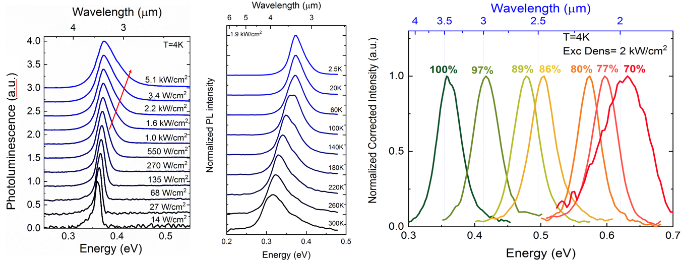
Figure on the right shows the measured photoluminescence, and its normalized intensity. The hex-Ge shells were grown on lattice-matching GaAs cores where the hex-Ge is grown at a temperature of 600 °C. On the far right its tunability covers a range from 1.8 to 4.2 µm.
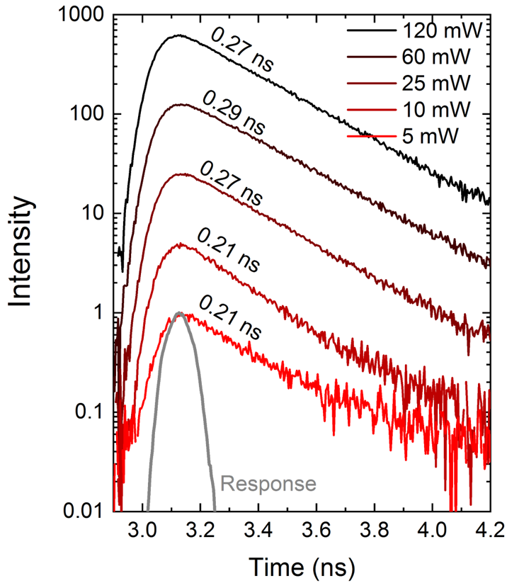
Finally, hex-SiGe is capable to operate in the radiative limit (absence of nonradiative losses) at room temperature, which is quite exceptional in comparison with many III-V semiconductors. This provides a first indication that the superiority of Si-based technology also applies to optical emission of Hex-SiGe.